FLEX
FLEX
FLEX Session 9: Developments in Printing & Other Additive Manufacturing
Mass production with AI-accelerated high-precision inkjet printing: NeuralJet™ Technology
Wednesday, July 10, 2024
2:30pm - 3:00pm PDT
Location: Moscone South, Level 3, Room 302

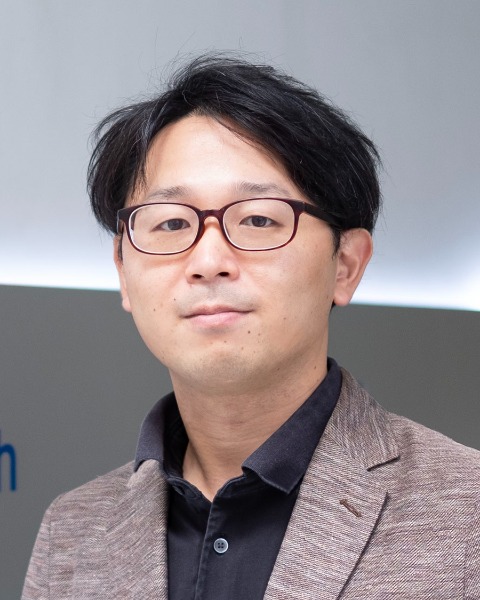
Masaaki Sugimoto
Board Director / Co-Founder
Elephantech Inc
Tokyo, Japan
Speaker (FLEX)(s)
Elephantech has been mass-producing electronic circuits with inkjet printing for four years. Shinya Shimizu, the CEO of Elephantech, will introduce the latest high-precision inkjet production technology.
In the domain of electronics manufacturing, the Subtractive method has long been foundational for printed circuit board (PCB) production. This well-established methodology relies on the preparation of large copper foils, which are then processed to retain only the necessary circuitry on the PCBs.
However, the seemingly efficient production of the subtractive method belies a substantial environmental drawback. The etching of substantial amounts of copper and photoresists required in the Subtractive method yields concentrated wastewater with notable environmental repercussions. This effluent not only poses direct environmental threats but also necessitates complex and energy-intensive treatment for safe disposal.
The environmental implications of PCB manufacturing have garnered attention in numerous studies. Kupka et al. (2018) employed "virtual product models" to propose a standard emission factor for PCBs at 212.48 kg-CO2/m2. With the PCB production volume estimated at 307 million m2 in 2021 based on data from Fuji Chimera Research Institute, Inc., this would correspond to a projected total emission of 66 million t-CO2 solely from PCB production.
In response to these environmental concerns, the industry has sought sustainable alternatives, with a shift towards dry processes using printed electronics technology, as opposed to traditional wet etching. Yet, this shift faces challenges, chiefly in ensuring product reliability — a paramount consideration in PCB manufacturing. This challenge has impeded a broad-based transition to mass production via dry processes.
Nevertheless, a promising advancement has been made by Elephantech Inc., which has commenced mass production of flex circuits using a semi-dry approach called “Pure-Additive™ method”.
This method integrates metal inkjet printing technology with electroless copper plating, whereby copper lines are printed onto a resin substrate and subsequently plated to increase thickness of the copper lines. The Pure-AdditiveTM method offers a sustainable alternative in electronics manufacturing.
Based on our analysis, the Pure-AdditiveTM method can reduce 75% of carbon footprint, 70% of copper usage and 95% of water consumption. In addition, this method does not require etching processes and avoids wastewater pollution.
Currently, the Pure-Additive™ method has been applied to the mass production of single-sided flexible circuits, with ongoing developments aimed at expanding its application to double-sided flexible circuits and PCBs with rigid substrates.
