SEMICON West
Advanced Manufacturing Processes
Driving The Next Generations Of Devices With Advanced Lithography, Heterogeneous Integration And Packaging
Powering the Scaling Roadmap with EUV Lithography
Thursday, July 11, 2024
1:55pm - 2:15pm PDT
Location: TechTALKS Stage, Moscone South, Exhibition Level, Room 7

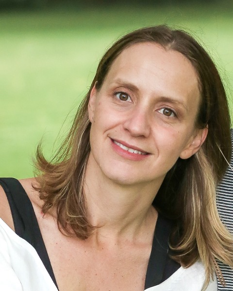
Luciana Meli, PhD
Senior Manager, Lithography and Metrology
IBM
Albany, New York, United States
Speaker (AdvMfg)(s)
Over the past two decades, with the plateauing of conventional device scaling, there has been a surge in material and device architecture innovations to meet the continuous demand for enhanced compute power. EUV Lithography (EUVL) is an integral enabler of this architecture innovations, affording both traditional scaling in the back end of the line (BEOL) and novel area cell scaling opportunities in the front end of the line (FEOL). The successful integration of EUVL in a way that enables design flexibility, simplification of mask assembly, and reduction of manufacturing complexity, needs to consider factors such as edge placement error (EPE) and stochastic effects inherent in EUVL. In this talk we will describe some unique ways we can leverage 0.33NA EUV lithography for scaling while addressing EPE and stochastic concerns. We will also explore the opportunities that the emergence of High Numerical Aperture (NA=0.55) EUVL can bring, proposing insertion points in the flow and addressing unique patterning challenges to harness this technology.
